
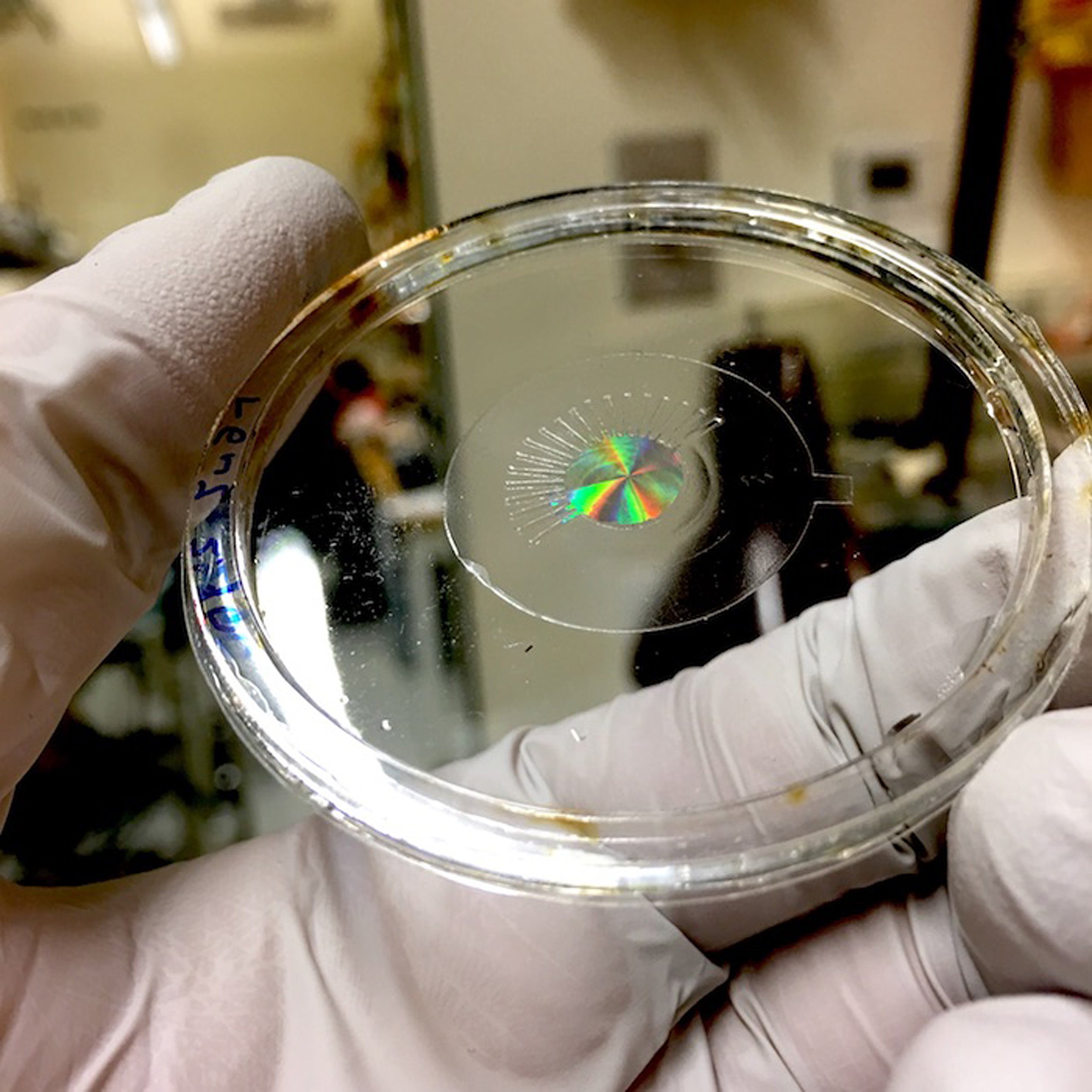
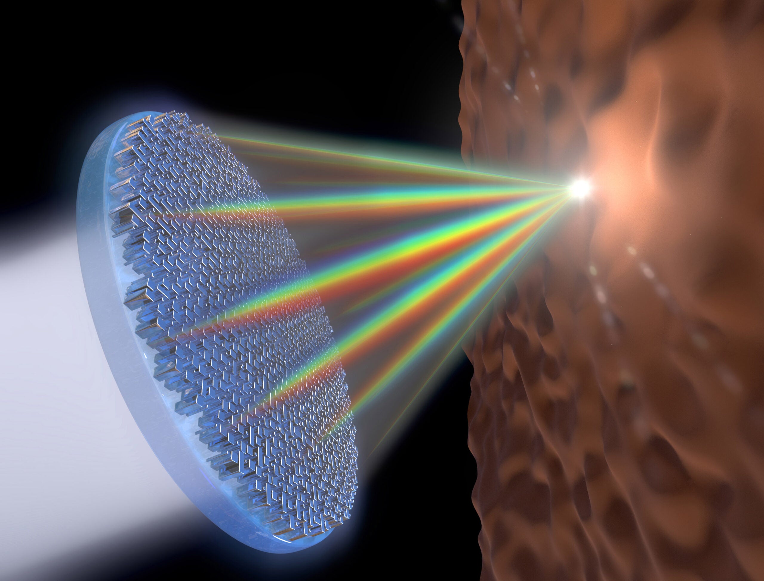
The metalens (made of silicon) are mounted on a transparent, stretchy polymer film, without any electrodes. The iridescence is produced by the large number of nanostructures within the metalens.
Alan She/ Harvard SEAS
Science & Tech
Breakthroughs seen in artificial eye and muscle technology
Adaptive metalens ‘can change its focus in real time, just like the human eye’
Inspired by the human eye, researchers at the Harvard John A. Paulson School of Engineering and Applied Sciences (SEAS) have developed an adaptive metalens that is essentially a flat, electronically controlled artificial eye. The adaptive metalens simultaneously controls for three of the major contributors to blurry images: focus, astigmatism, and image shift.
The research is published in Science Advances.
“This research combines breakthroughs in artificial muscle technology with metalens technology to create a tunable metalens that can change its focus in real time, just like the human eye,” said Alan She, an SEAS graduate student at the Graduate School of Arts and Sciences, and first author of the paper. “We go one step further to build the capability of dynamically correcting for aberrations such as astigmatism and image shift, which the human eye cannot naturally do.”
“This demonstrates the feasibility of embedded optical zoom and autofocus for a wide range of applications, including cell phone cameras, eyeglasses, and virtual and augmented reality hardware,” said Federico Capasso, the Robert L. Wallace Professor of Applied Physics and Vinton Hayes Senior Research Fellow in Electrical Engineering at SEAS and senior author of the paper. “It also shows the possibility of future optical microscopes, which operate fully electronically and can correct many aberrations simultaneously.”
The Harvard Office of Technology Development has protected the intellectual property relating to this project and is exploring commercialization opportunities.
To build the artificial eye, the researchers first needed to scale up the metalens.
Metalenses focus light and eliminate spherical aberrations through a dense pattern of nanostructures, each smaller than a wavelength of light. Earlier metalenses were about the size of a single piece of glitter.
“Because the nanostructures are so small, the density of information in each lens is incredibly high,” said She. “If you go from a 100 micron-size lens to a centimeter-size lens, you will have increased the information required to describe the lens by 10,000. Whenever we tried to scale up the lens, the file size of the design alone would balloon up to gigabytes or even terabytes.”
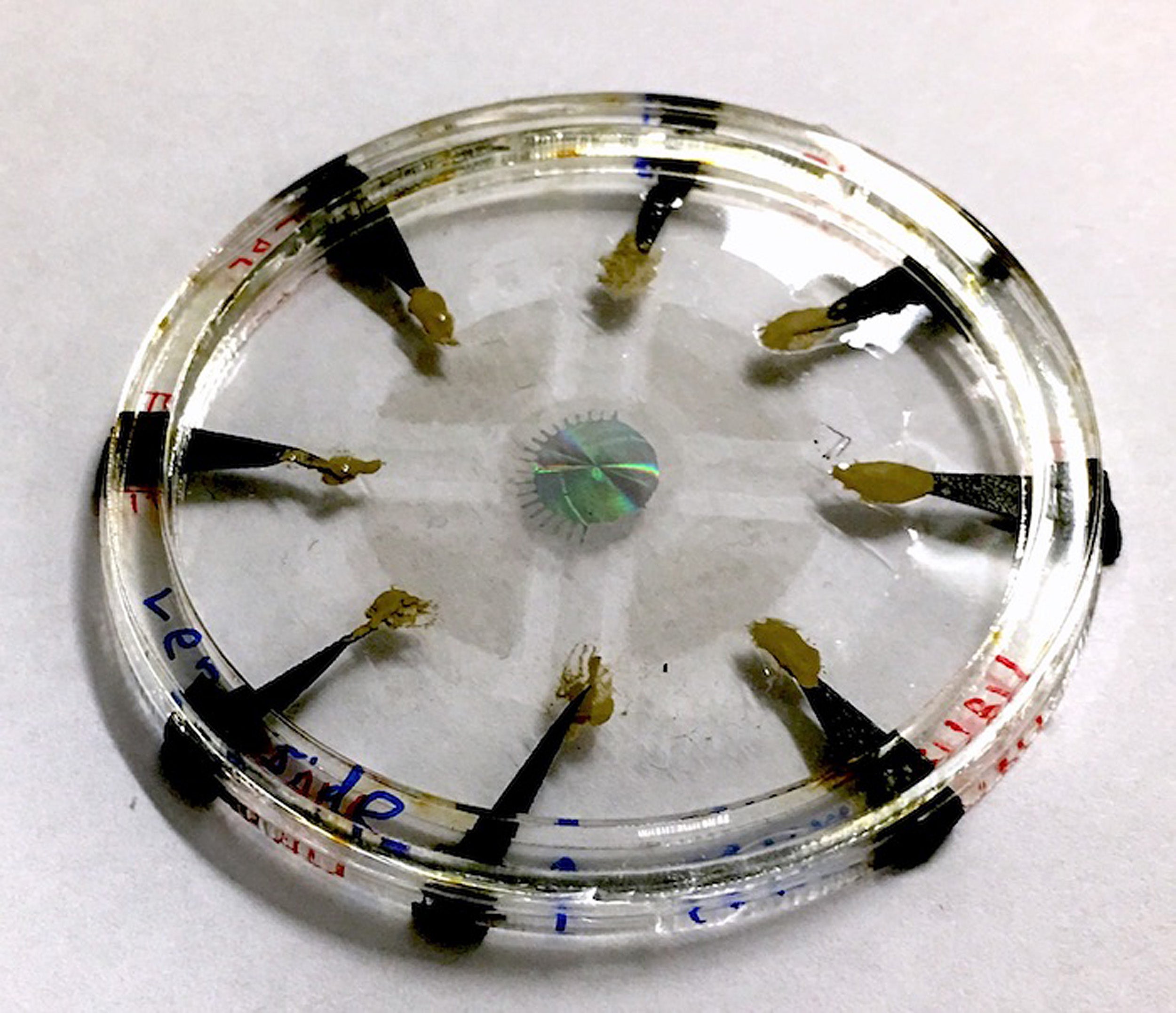
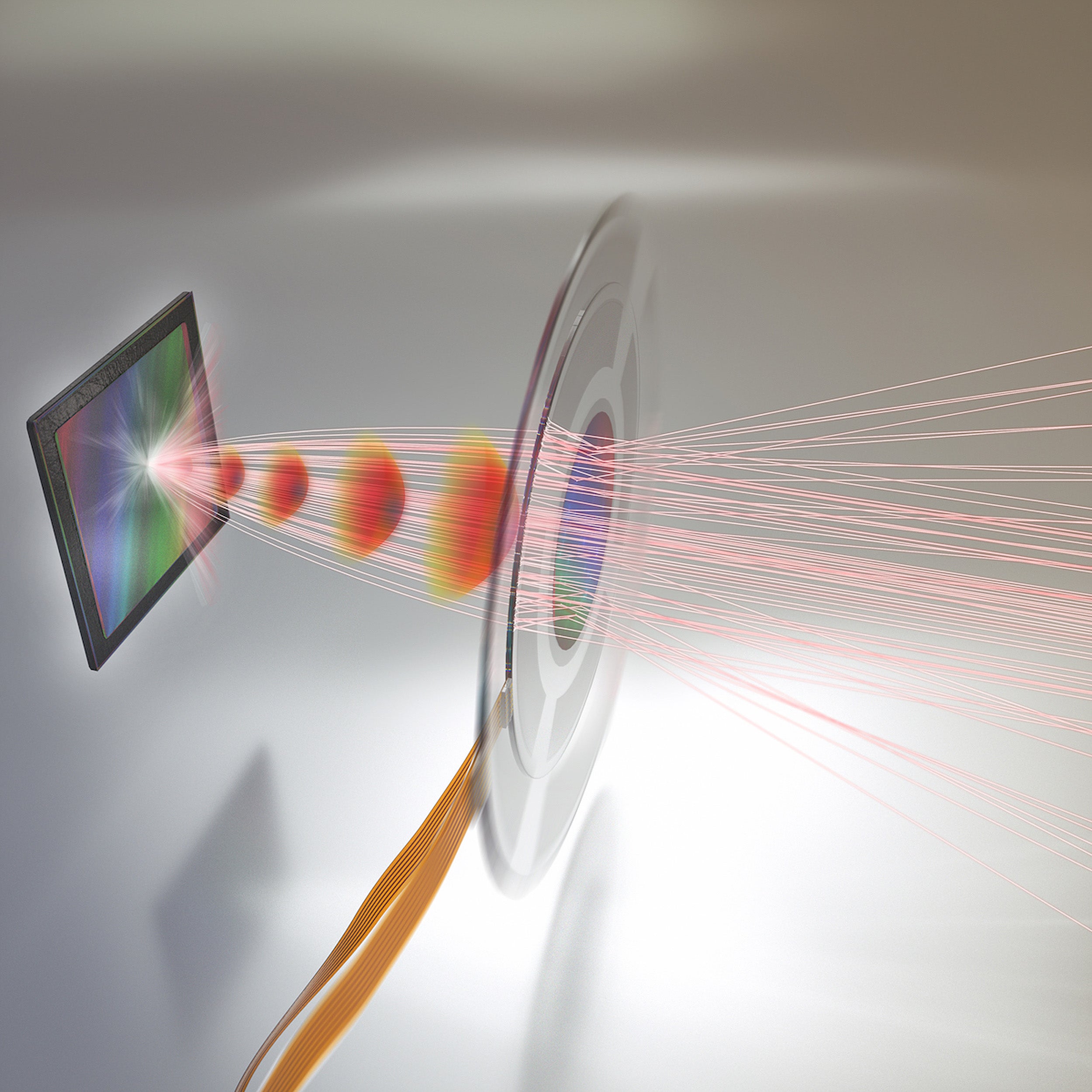
Image 1: The actual device, in which the adaptive metalens (center) is controlled by embedded electrodes made of carbon nanotubes. Image 2: The adaptive metalens focuses light rays onto an image sensor. An electrical signal controls the shape of the metalens to produce the desired optical wavefronts (shown in red), resulting in better images.
Alan She/ Harvard SEAS
To solve this problem, the researchers developed a new algorithm to shrink the file size to make the metalens compatible with the technology currently used to fabricate integrated circuits. In a paper recently published in Optics Express, the researchers demonstrated the design and fabrication of metalenses of up to centimeters or more in diameter.
“This research provides the possibility of unifying two industries, semiconductor manufacturing and lens-making, whereby the same technology used to make computer chips will be used to make metasurface-based optical components, such as lenses,” said Capasso.
Next, the researchers needed to adhere the large metalens to an artificial muscle without compromising its ability to focus light. In the human eye, the lens is surrounded by ciliary muscle, which stretches or compresses the lens, changing its shape to adjust its focal length. Capasso and his team collaborated with David Clarke, Extended Tarr Family Professor of Materials at SEAS and a pioneer in the field of engineering applications of dielectric elastomer actuators, also known as artificial muscles.
The researchers chose a thin, transparent dielectric elastomer with low loss — meaning light travels through the material with little scattering — to attach to the lens. To do so, they needed to develop a platform to transfer and adhere the lens to the soft surface.
“Elastomers are so different in almost every way from semiconductors that the challenge has been how to marry their attributes to create a novel multifunctional device and, especially, how to devise a manufacturing route,” said Clarke. “As someone who worked on one of the first scanning electron microscopes (SEMs) in the mid-1960s, it is exhilarating to be a part of creating an optical microscope with the capabilities of an SEM, such as real-time aberration control.”
The elastomer is controlled by applying voltage. As it stretches, the position of nanopillars on the surface of the lens shift. The metalens can be tuned by controlling both the position of the pillars in relation to their neighbors and the total displacement of the structures. The researchers also demonstrated that the lens can simultaneously focus, control aberrations caused by astigmatisms, and perform image shift.
Together, the lens and muscle are only 30 microns thick.
“All optical systems with multiple components — from cameras to microscopes and telescopes — have slight misalignments or mechanical stresses on their components, depending on the way they were built and their current environment, that will always cause small amounts of astigmatism and other aberrations, which could be corrected by an adaptive optical element,” said She. “Because the adaptive metalens is flat, you can correct those aberrations and integrate different optical capabilities onto a single plane of control.”
Next, the researchers aim to further improve the functionality of the lens and decrease the voltage required to control it.
The research was co-authored by Shuyan Zhang and Samuel Shian. The research was supported in part by the Air Force Office of Scientific Research and by the National Science Foundation. This work was performed in part at the Center for Nanoscale Systems (CNS), which is supported by the National Science Foundation.